
Add to Cart
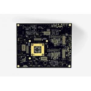
What is the Application of PCB?
With the shift of industry from analog to digital. The mass production of PCB has been stimulated. From the radio, TV, and tape recorder, to the walkman, calculators, computers, laptops, and SPC exchanges. With the high development of electronic products, it's hard to do the same way that used 3C to define the PCB,
What are the application fields of printed Circuit boards?
Mobile phones, microwaves, Consumer Electronics, communications, network base stations, hybrid integrated circuits, and home fans.
What certificates and capacity does ABIS have?
We have ISO14001, ISO9001, UL, and so on.
| Raw material | FR-4, High TG FR-4, PTFE, Aluminum Base, Cu base. Rogers, etc |
| Board Thickness | 0.20mm--8.00mm |
| Layer | 1 Layer-20 Layer |
| Insulation Layer Thickness | 0.075mm--5.00mm |
| Min.hole size | 0.1mm (drilling hole) |
| Max. Board size | 200mm*600mm |
| Out Layer Copper Thickness | 18um--350um |
| Inner Layer Copper Thickness | 17um--175um |
| NPTH Hole Tolerance | +/- 0.075mm |
| PTH hole Tolerance | +/-0.05mm |
| Outline tolerance | +/-0.13mm |
| Surface finished | HASL, ENIG, Chem. Tin, Flash Gold, OSP, Gold finger |
| Solder Mask Type | LPI |
| Others | RFQ. |
What is your Lead Time?
Category | Q/T Lead time | Standard Lead Time | Mass Production | |||
2 Layers | 24hrs | 3-4 working days | 8-15 working days | |||
4 Layers | 48hrs | 3-5 working days | 10-15 working days | |||
6 Layers | 72hrs | 3-6 working days | 10-15 working days | |||
8 Layers | 96hrs | 3-7 working days | 14-18 working days | |||
10 Layers | 120hrs | 3-8 working days | 14-18 working days | |||
12 Layers | 120hrs | 3-9 working days | 20-26 working days | |||
14 Layers | 144hrs | 3-10 working days | 20-26 working days | |||
16-20 Layers | Depends on the specific requirements | |||||
20+ Layers | Depends on the specific requirements | |||||


