
SMD Soldering 0.075mm 2OZ Custom PCB Assembly
Brand Name:OEM/ODM
Certification:UL, Rohs
Model Number:SL00710S01
Minimum Order Quantity:Negotiable
Delivery Time:7-12 days
Payment Terms:L/C, T/T, Western Union, MoneyGram
Contact Now
Add to Cart
Verified Supplier
Location:
Shenzhen Guangdong China
Address:
Chengda Business Center, Rongfu Road, Fucheng Street, Longhua District, Shenzhen
Supplier`s last login times:
within 25 hours
Product Details
Company Profile
Product Details
PCB Assembly Wireless PCBA custom circuit board smd soldering assembly
This PCBA Board is assembled with FR - 4 made bare pcb board and the board thickness is 1.6 mm, copper thickness is normally 1OZ / 35 µm. Immersion gold surface treatment make the PCBa work longer and more eco-friendly. We need Gerber File & BOM List to produce your PCBa assembly order.
Files Requested For PCB Assembly Quotation
---In order to provide you with the most efficient and accurate
quote on manufacturing the requested unit, we ask that you provide
us with the following information.
1. Gerber file,PCB file,Eagle file or CAD file are all acceptable
2. A detailed bill of materials (BOM)
3. Clear pictures of PCB or PCBA sample for us
4. Quantity and delivery required
5. Test method for PCBA to guarantee 100% good quality products.
6. Schematics file for PCB design if need to do function test.
7. A sample if available for better sourcing
8. CAD files for enclosure manufacturing if required
9. A complete wiring and assembly drawing showing any special
assembly instructions if required
Shinelink kinds PCBA product
94V0 PCBA manufacture Scale capabilities up to
We combine advanced processes with highly skilled resources.
Keeping up with the leading advanced technology and management
system in One-stop services of PCB assembly
SMT process (RoHs Compliant) Capabilities up to:
1. 0201 Chip Size
2. 12 mils Integrated Circuit (IC) Pitch
3. Micro Ball Grid Array (BGA) – Pitch 16 mils
4. Flip Chip (Controlled Collapse Chip Connection) – Pitch 5 mils
5. Quad Flat Package (QFP) – Pitch 12 mils
THT(Wave soldering) process (RoHs Compliant) Capabilities up to:
1.Single side wave soldering
2.SMT & THT mixture process
PCB Assembly Capabilities
| Turnkey PCBA | PCB+components sourcing+assembly+package |
| Assembly details | SMT and Thru-hole, ISO lines |
| Lead Time | Prototype: 15 work days. Mass order: 20~25 work days |
| Testing on products | Flying Probe Test, X-ray Inspection, AOI Test, functional test |
| Quantity | Min quantity: 1pcs. Prototype, small order, mass order, all OK |
| Files we need | PCB: Gerber files(CAM, PCB, PCBDOC) |
| Components: Bill of Materials(BOM list) | |
| Assembly: Pick-N-Place file | |
| PCB panel Size | Min size: 0.25*0.25 inches(6*6mm) |
| Max size: 20*20 inches(500*500mm) | |
| PCB Solder Type | Water Soluble Solder Paste, RoHS lead free |
| Components details | Passive Down to 0201 size |
| BGA and VFBGA | |
| Leadless Chip Carriers/CSP | |
| Double-sided SMT Assembly | |
| Fine Pitch to 0.8mils | |
| BGA Repair and Reball | |
| Part Removal and Replacement | |
| Component package | Cut Tape,Tube,Reels,Loose Parts |
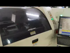
| PCB assembly process | Drilling-----Exposure-----Plating-----Etaching & Stripping-----Punching-----Electrical Testing-----SMT-----Wave Soldering-----Assembling-----ICT-----Function Testing-----Temperature & Humidity Testing |
PCBA Picture
FAQ:
1. What kinds of boards can Shinelink process?
Common FR4, high-TG and halogen-free boards, Rogers, Arlon, Telfon, aluminum/copper-based boards, PI, etc.
2. What data are needed for PCB & PCBA production?
2.1 BOM (Bill of Materials) with reference designators: component
description, manufacturer’s name and part number.
2.2 PCB Gerber files.
2.3 PCB fabrication drawing and PCBA assembly drawing.
2.4 Test procedures.
2.5 Any mechanical restrictions such as assembly height
requirements.


SMD Soldering 0.075mm 2OZ Custom PCB Assembly
Inquiry Cart
0