Product Details
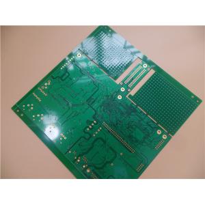
Via in Pad PCB High Temperature VIP PCB 8-Layer Circuit Board on
FR-4 with Immersion Gold for Satellite Radio
1.1 General description
This is a type of 8 layer printed circuit board built on FR-4 Tg170
substrate for the application of Satellite Radio. It's 1.6 mm thick
with white silkscreen(Taiyo) on green solder mask (Taiyo) and
immersion gold on pads. The base material is from Taiwan ITEQ
supplying 1 up PCB per panel. Vias with 0.2mm are resin filled and
capped (via in pad). They're fabricated per IPC 6012 Class 2 using
supplied Gerber data. Each 25 panels are packed for shipment.
1.2 Features and benefits
(1) RoHS compliant and suitable for high thermal reliability needs
(2) High solderability, no stressing of circuit boards and less
contamination of PCB surface.
(3) Delivery on time. Higher than 98% on-time-delivery rate.
(4) 30000 square meter month capability
(5) More than 15 years of experience
(6) Volume Production capability
1.3 Applications
(1) Satellite Communication
(2) Solar Panel Inverter
(3) Embedded Processor
1.4 Parameter and data sheet
| PCB SIZE | 215 x 212mm=1PCS |
| BOARD TYPE | Multilayer PCB |
| Number of Layers | 8 layers |
| Surface Mount Components | YES |
| Through Hole Components | YES |
| LAYER STACKUP | copper ------- 18um(0.5oz)+plate TOP layer |
| Prepreg 7628(43%) 0.195mm |
| copper ------- 35um(1oz) MidLayer 1 |
| FR-4 0.2mm |
| copper ------- 35um(1oz) MidLayer 2 |
| Prepreg 7628(43%) 0.195mm |
| copper ------- 35um(1oz) MidLayer 3 |
| FR-4 0.2mm |
| copper ------- 35um(1oz) MidLayer 4 |
| Prepreg 7628(43%) 0.195mm |
| copper ------- 35um(1oz) MidLayer 5 |
| FR-4 0.2mm |
| copper ------- 35um(1oz) MidLayer 6 |
| Prepreg 7628(43%) 0.195mm |
| copper ------- 18um(0.5oz)+plate BOT Layer |
| TECHNOLOGY | |
| Minimum Trace and Space: | 4mil/4mil |
| Minimum / Maximum Holes: | 0.3/3.2mm |
| Number of Different Holes: | 18 |
| Number of Drill Holes: | 11584 |
| Number of Milled Slots: | 2 |
| Number of Internal Cutouts: | 0 |
| Impedance Control: | no |
| Number of Gold finger: | 0 |
| BOARD MATERIAL | |
| Glass Epoxy: | FR-4 TG170℃, er<5.4.IT-180, ITEQ Supplied |
| Final foil external: | 1oz |
| Final foil internal: | 1oz |
| Final height of PCB: | 1.6mm ±0.16 |
| PLATING AND COATING | |
| Surface Finish | Immersion gold (32.1% ) 0.05µm over 3µm nickel |
| Solder Mask Apply To: | TOP and Bottom, 12micron Minimum |
| Solder Mask Color: | Green, PSR-2000 KX700G, Taiyo Supplied. |
| Solder Mask Type: | LPSM |
| CONTOUR/CUTTING | Routing, stamp holes. |
| MARKING | |
| Side of Component Legend | TOP and Bottom. |
| Colour of Component Legend | White, S-380W, Taiyo Supplied. |
| Manufacturer Name or Logo: | Marked on the board in a conductor and leged FREE AREA |
| VIA | plated through hole(PTH), minimum size 0.3mm. |
| FLAMIBILITY RATING | UL 94-V0 Approval MIN. |
| DIMENSION TOLERANCE | |
| Outline dimension: | 0.0059" |
| Board plating: | 0.0029" |
| Drill tolerance: | 0.002" |
| TEST | 100% Electrical Test prior shipment |
| TYPE OF ARTWORK TO BE SUPPLIED | email file, Gerber RS-274-X, PCBDOC etc |
| SERVICE AREA | Worldwide, Globally. |
1.5 Design For Manufacture (3)
| Serial NO. | Procedure | Item | Manufacturing capability |
| Large volume (S<100 m²) | Middle volume (S<10 m²) | Prototype(S<1m²) |
|
| 31 | Solder mask (18um, 35um, 70um etc are finished copper. If not
mentioned copper, finished 1oz is the default value ) | Maximum via-plug diameter | 0.5mm | 0.5mm | 0.5mm |
| 32 | Min.width of solder mask bridge | Green:5mil(35um) | Green:4mil(35um) | Green:4mil(35um) |
| 33 | Yellow:5mil(35um) | Yellow:4mil(35um) | Yellow:4mil(35um) |
| 34 | Blue:5mil(35um) | Blue:4mil(35um) | Blue:4mil(35um) |
| 35 | Black:6mil(35um) | Black:6mil(35um) | Black:6mil(35um) |
| 36 | White:6mil(35um) | White:6mil(35um) | White:6mil(35um) |
| 37 | All of Matt:6mil | All of Matt:6mil | All of Matt:6mil |
| 38 | Green:5mil(70um) | Green:4mil(70um) | Green:4mil(70um) |
| 39 | Yellow:5mil(70um) | Yellow:4mil(70um) | Yellow:4mil(70um) |
| 40 | Blue:5mil(70um) | Blue:4mil(70um) | Blue:4mil(70um) |
| 41 | Black:6mil(70um) | Black:6mil(70um) | Black:6mil(70um) |
| 42 | White:6mil(70um) | White:6mil(70um) | White:6mil(70um) |
| 43 | Open solder mask | 4mil(35um) | 4mil(35um) | 3mil(35um) |
| 44 | Solder mask coverage | 4mil(35um) | 4mil(35um) | 3mil(35um) |
| 45 | Min.width of solder mask text | 9mil(35um) | 9mil(35um) | 8mil(35um) |
| 46 | Min.thickness of Solder mask | 9um(35um) | 9um(35um) | 9um(35um) |
| 47 | Max.thickness of solder mask | 30um(35um) | 30um(35um) | 30um(35um) |
Company Profile
Company Profile
Founded in 2003, Shenzhen Bicheng Electronics Technology Co., Ltd is an established high frequency PCB supplier and exporter in
Shenzhen China, severing cellular base station antenna, satellite,
high frequency passive components, microstrip line and band line
circuit, millimeter wave equipment, radar systems, digital radio
frequency antenna and other fields worldwide for 18 years. Our high
frequency PCBs are mainly built on 3 high frequency material
brands: Rogers Corporation, Taconic and Wangling. Dielectric
constant ranges from 2.2 to 10.2 etc.
Bicheng PCB is headquartered in Shenzhen, a city with great
economic vitality. Based in China, we adhere to the philosophy of
servicing small and medium sized companies offering variety of
circuit boards to meet the demands of market.
Main Business & PCB Applications
We maintain the highest standards which support products that
exhibit exceptional quality, performance and reliability. We also have divisions of FR-4 circuit board, flexible circuits
and metal core PCBs featured as prototypes, small runs to mass
production. We actively research and build such high value added
PCB projects as HDI, quick turn, impedance control, heavy copper
and backplane board etc. This has made our PCB products generate an
effective prolongation and complementation, as well as formation of
integrated products line ranging from low-end to high-end.The circuit boards are used in the industries of home appliances,
portable and consumable electronics, medical filed, aerospace as
well as telecommunications etc.
Main Material Partners