
Add to Cart
Features:
² Compliant to INF-8077-XFP MSA
² Data Rate from 9.95 Gbps to 11.3Gbps
² 1330nm DFB Transmitter, PIN Photodiode and TIA
² SM 9/125um up to 20Km
² Simplex LC connector
² Built-in digital diagnostic monitoring functions
² All-Metal housing for superior EMI Performance
² Power dissipation < 1.5W, Single 3.3V power supply
² Operating Case Temperature Standard: 0℃~+70℃
² Protocol-independent,XFI Interface
² Hot Pluggable
² ROHS6 Compliant
Applications
² SONET OC-192 SR-1&SDH STM I-64.1
² 10GBASE-LR/LW 10Gigabit Ethernet
² 10G Fiber Channel
Description:
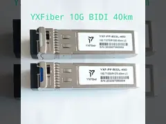
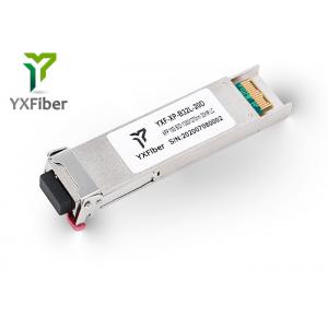
YXF-XP-B32L-20D is hot pluggable 3.3V Small-Form-Factor transceiver module. It designed expressly for high-speed communication applications that require rates up to 11.3Gb/s, it designed to be compliant with XFP MSA. The module data link up to 20Km in 9/125um single mode fiber.The optical output can be disabled by a LVTTL logic high-level input of Tx Disable. Loss of signal (LOS) output is provided to indicate the loss of an input optical signal of receiver or the link status with partner.
Specifications:
| Technical Parameters | Descriptions | Technical Parameters | Descriptions |
| Model Number | YXF-XP-B32L-20D | Interface | LC |
| Fiber type | SMF | Laser/Detector | DFB/PIN |
| Form Factor | BIDI SFP | DDM | Yes |
| Data Rate | 10Gbps | Output Power | 1~-6dBm |
| Wavelength | 1330nm/1270nm | Power Supply | 3.3V |
| Distance | 20KM | Temperature | 0~70°C |
| Sensitivity | <-14.0dBm | Certificate | CE,ROHS,FCC,ISO9001,SGS |
| Selling Units | Single | Warranty | 1Year |
Electrical Characteristics
| Parameter | Symbol | Min. | Typ. | Max. | Unit | Notes |
| Transmitter | ||||||
| Input differential impedance | Ri | 100 | Ω | 1 | ||
| Differential data input swing | Vin,pp | 120 | 820 | mV | ||
| Transmit disable voltage | VD | 2 | VCC3 | V | ||
| Transmit enable voltage | VEN | Vee | Vee+0.8 | V | ||
| Data dependent input jitter | DDJ | 0.1 | U | |||
| Data input Total Jitter | TJ | 0.28 | U | |||
| Receiver | ||||||
| Differential data output swing | Vout,pp | 300 | 850 | mV | ||
| Data output rise time,fall time | tr | 24 | P | 2 | ||
| Los Fault | VLOS fault | 2 | VCC3host | V | 3 | |
| Los Normal | VLOS norm | Vee | Vee+0.8 | V | 3 | |
| Total Jitter | TJ | 0.70 | U | |||
| Deterministic Jitter | DJ | 0.42 | U | |||
Notes:
1. Connected directly to TX data input pins, AC coupling from pins into laser drive
2. 20 – 80 % . Measured with Module Compliance Test Board and OMA test pattern. Use of four 1’s and four 0’s in sequence in the PRBS^9 is an acceptable alternative.
3. LOS is an open collector output. Should be pulled up with 4.7kΩ – 10kΩ on the host board. Normal operation is logic 0; loss of signal is logic 1. Maximum pull-up voltage is 3.6V