
Add to Cart
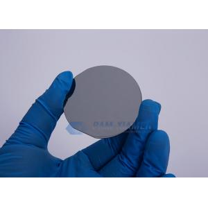
Undoped InSb Wafer, 2”, As-Cut Wafer, Mechanical Wafer, Or Polished
Wafer
PAM-XIAMEN provides single crystal InSb(Indium Antimonide) wafer growth by Liquid Encapsulated Czochralski ( LEC ) method. Indium Antimonide (InSb) can be supplied as wafers with as-cut, etched or polished finishes and are available in a wide range of carrier concentration, diameter and thickness.PAM-XIAMEN can provide epi ready grade InSb wafer for your MOCVD & MBE epitaxial application .
Undoped InSb Wafer, 2”, As-Cut Wafer, Mechanical Wafer, Or Polished Wafer
Please contact our engineer team for more wafer information.
| Wafer Specification | |
| Item | Specifications |
| Wafer Diameter | 2″50.5±0.5mm |
| Crystal Orientation | 2″(111)AorB±0.1° |
| Thickness | 2″625±25um |
| Primary flat length | 2″16±2mm |
| Secondary flat length | 2″8±1mm |
| Surface Finish | P/E, P/P |
| Package | Epi-Ready,Single wafer container or CF cassette |
| Electrical and Doping Specification | |
| Conduction Type | n-type |
| Dopant | Undoped |
| EPD cm-2 | ≤50 |
| Mobility cm² V-1s-1 | ≥4*105 |
| Carrier Concentration cm-3 | 5*1013-3*1014 |
Band structure and carrier concentration of InSb Wafer
Band structure and carrier concentration of InSb Wafer include Basic Parameters,Temperature, Dependences,Dependence of the Energy Gap on Hydrostatic Pressure, Effective Masses, Donors and Acceptors
Basic Parameters
Temperature Dependences
Dependence of the Energy Gap on Hydrostatic Pressure
Effective Masses
Donors and Acceptors
| Energy gap | 0.17 eV |
| Energy separation (EΓL) between Γ and L valleys | 0.51 eV |
| Energy separation (EΓX) between Γ and X valleys | 0.83 eV |
| Energy spin-orbital splitting | 0.80 eV |
| Intrinsic carrier concentration | 2·1016 cm-3 |
| Intrinsic resistivity | 4·10-3 Ω·cm |
| Effective conduction band density of states | 4.2·1016 cm-3 |
| Effective valence band density of states | 7.3·1018 cm-3 |
| Band structure and carrier concentration of InSb 300 K Eg = 0.17 eV EL = 0.68 eV EX= 1.0 eV Eso = 0.8 eV |
Eg = 0.24 - 6·10-4·T2/(T+500) (eV),
where T is temperatures in degrees K (0 < T < 300).
Nc~ 8·1012·T3/2 (cm-3)
Nn ~ 1.4·1015·T3/2 (cm-3).
ni = (Nc·Nν)1/2exp(-Eg/(2kbT))
For 200K < T < 800 K ni = 2.9·1011(2400 - T)3/4
·(1+2.7·10-4·T)·T3/2 ·exp(-(0.129 - 1.5·10-4T)/(2kbT)) (cm-3)
| The temperature dependences of the intrinsic carrier concentration. | |
| Fermi level versus temperature for different concentrations of shallow donors and acceptors. |
Eg≈Eg(0) + 13.7·10-3P - 3.6·10-5P2 (eV)
EL≈EL(0) + 4.7·10-3P - 1.1·10-5P2 (eV)
EX≈EX(0) - 3.5·10-3P + 0.64·10-5P2 (eV),
where P is pressure in kbar.
| Electrons: | |
| For Γ-valley | mΓ = 0.0.14mo |
| Non-parabolicity: E(1+αE) = h2k2/(2mΓ) | α = 4.1 (eV-1) |
| In the L-valley effective mass of density of states | mL=0.25mo |
| Electron effective mass versus electron concentration |
| Holes: | mh = 0.43mo |
| Heavy | mh = 0.43mo |
| Light | mlp = 0.015mo |
| Split-off band | mso = 0.19mo |
| Effective mass of density of states | mv = 0.43mo |
Se, S, Te.
| Cd | Zn | Cr | Cu° | Cu- |
| 0.01 | 0.01 | 0.07 | 0.028 | 0.056 |
Are You Looking for an InSb substrate?
PAM-XIAMEN is proud to offer indium phosphide substrate for all different kinds of projects. If you are looking for InSb wafers, send us enquiry today to learn more about how we can work with you to get you the InSb wafers you need for your next project. Our group team is looking forward to providing both quality products and excellent service for you!

