
Add to Cart
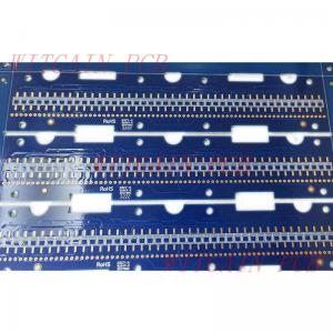
Double Layer FR4 Substrate Material PCB Blue Solder Mask Ink
1 2 Layer FR4 substrate material printed circuit board.
2 ROHS, MSDS, SGS, UL, ISO9001&ISO14001 Certificated.
3 FR4 TG150 material, pcb thickness is 1.6mm.
4 Blue solder mask and white silkscreen.
5 35um copper on each layer.
6 Quality Acceptance Standards: IPC 6012E Class2
7 Surface treatment is immersion gold 1u'.
8 Customized pcb, need customer to send us the gerber file or pcb file.
| S1150G | |||||
| Items | Method | Condition | Unit | Typical Value | |
| Tg | IPC-TM-650 2.4.25 | DSC | ℃ | 155 | |
| Td | IPC-TM-650 2.4.24.6 | 5% wt. loss | ℃ | 380 | |
| CTE (Z-axis) | IPC-TM-650 2.4.24 | Before Tg | ppm/℃ | 36 | |
| After Tg | ppm/℃ | 220 | |||
| 50-260℃ | % | 2.8 | |||
| T260 | IPC-TM-650 2.4.24.1 | TMA | min | >60 | |
| T288 | IPC-TM-650 2.4.24.1 | TMA | min | 30 | |
| Thermal Stress | IPC-TM-650 2.4.13.1 | 288℃, solder dip | -- | pass | |
| Volume Resistivity | IPC-TM-650 2.5.17.1 | After moisture resistance | MΩ.cm | 6.4 x 10⁷ | |
| E-24/125 | MΩ.cm | 5.3 x 10⁶ | |||
| Surface Resistivity | IPC-TM-650 2.5.17.1 | After moisture resistance | MΩ | 4.8 x 10⁷ | |
| E-24/125 | MΩ | 2.8 x 10⁶ | |||
| Arc Resistance | IPC-TM-650 2.5.1 | D-48/50+D-4/23 | s | 140 | |
| Dielectric Breakdown | IPC-TM-650 2.5.6 | D-48/50+D-4/23 | kV | 45+kV NB | |
| Dissipation Constant (Dk) | IPC-TM-650 2.5.5.9 | 1MHz | -- | 4.8 | |
| IEC 61189-2-721 | 10GHz | -- | — | ||
| Dissipation Factor (Df) | IPC-TM-650 2.5.5.9 | 1MHz | -- | 0.01 | |
| IEC 61189-2-721 | 10GHz | -- | — | ||
| Peel Strength (1Oz HTE copper foil) | IPC-TM-650 2.4.8 | A | N/mm | — | |
| After thermal Stress 288℃,10s | N/mm | 1.4 | |||
| 125℃ | N/mm | 1.3 | |||
| Flexural Strength | LW | IPC-TM-650 2.4.4 | A | MPa | 600 |
| CW | IPC-TM-650 2.4.4 | A | MPa | 450 | |
| Water Absorption | IPC-TM-650 2.6.2.1 | E-1/105+D-24/23 | % | 0.1 | |
| CTI | IEC60112 | A | Rating | PLC 0 | |
| Flammability | UL94 | C-48/23/50 | Rating | V-0 | |
| E-24/125 | Rating | V-0 | |||
Q1: What is a PCB Trace?
A1:
A PCB trace is a highly conductive track that is used to connect components on a Printed Circuit Board to each other. Since a PCB Trace is used to conduct electricity it has to be made of a material that is highly conductive and stable. Additionally, the physical properties like its width and thickness help determine the amount of current that can pass through managing thermal stability. The most popular material for making trace is Copper. PCB traces are a fundamental building block a PCB without which it would not be able to function. A Properly designed PCB trace is of absolute importance as it will determine the proper functioning of PCBs used in electronic devices.
There are a number of parameters that must be considered when designing PCB traces. The primary parameters that need to be considered are as follows:
Trace Width & Thickness:
The trace width and thickness are important design parameters for a PCB. These parameters determine the amount of current that can pass through the trace without overheating and damaging the board. The ability of the PCB to handle high levels of power requires a trace with high cross-sectional area.
The thickness of a trace in a PCB board is essential for a designer during the design process of a printed circuit board. It must be consistent throughout the PCB i.e the default thickness for PCBs can be between 1oz (35 microns) to 2oz (70 microns). Due to the variety of PCB boards (single-sided, double-sided, and multi-layered) available in the market, the trace thickness varies with the board type.
If these parameters are ignored the PCB board might not function as intended and result in damage or sparks which will harm the components connected to the board.
Trace Resistance
PCB Trace resistance is another design parameter that needs to be considered while designing a PCB. The PCB trace resistance is helpful in determining the loss in signal transfer though a PCB and how much power can be dissipated by the trace. If not factored correctly, this can lead to various design and implementation issues.
The Formula to calculate trace resistance is as follows:
Here L, W, and T represent the physical area of the trace, i.e., length, width, and height and α represents the temperature coefficient of the copper. The calculations can only determine an approximate value.
The primary issue of trace resistance is power loss. It will eventually lead to a temperature rise and a reduction in conductivity. The most efficient way to tackle power loss due to trace resistance is to increase the trace area (width & thickness) for which knowing the trace resistance is absolutely essential.
Trace Current
The current capacity of a PCB trace is the maximum current that can run through the trace without causing harm to any of the electronic components present on the board. The trace current of a PCB depends upon the trace width and thickness.


