
Add to Cart
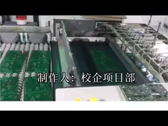
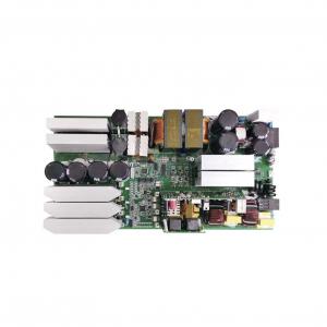
Wifi Module Panel Turnkey PCB Assembly Connector Circuit Board Soldering
PCB Process - Introduction to HDI
HDI (High Density Interconnect): High-density interconnection
technology, mainly using micro-blind / buried vias (blind / buried
vias), a technology that makes PCB circuit board circuit
distribution density higher. The advantage is that it can greatly
increase the usable area of the Turnkey PCB Assembly, making the
product as miniaturized as possible. However, due to the increase
in line distribution density, it is impossible to use traditional
drilling methods to drill through holes, and some of the via holes
must be drilled with laser drilling to form blind holes, or
cooperate with inner-layer buried vias to interconnect.
Generally, the diameter of the laser drilling hole is designed to be 3 ~ 4 mil (about 0.076 ~ 0.1 mm), and the insulation thickness between each laser drilling layer is about 3 mil. Due to the use of laser drilling many times, the key to the quality of the Turnkey PCB Assembly is the hole pattern after laser drilling and whether the hole can be evenly filled after the subsequent electroplating and filling.
Specification
| Article | Description | Capability |
| Material | Laminate materials | FR4, High TG FR4, High Frequency, Alum, FPC... |
| Board Cutting | Number of layers | 1-48 |
| Min.thickness for inner layers (Cu thickness are excluded) | 0.003”(0.07mm) | |
| Board Thickness | Standard | (0.1-4mm±10%) |
| Min. | Single/Double:0.008±0.004” | |
| 4layer:0.01±0.008” | ||
| 8layer:0.01±0.008” | ||
| Bow and twist | no more than 7/1000 | |
| Copper Weight | Outer Cu weight | 0.5-4 0z |
| Inner Cu weight | 0.5-3 0z | |
| Drilling | Min size | 0.0078”(0.2mm) |
| Drill deviation | ±0.002″(0.05mm) | |
| PTH hole tolerance | ±0.002″(0.005mm) | |
| NPTH hole tolerance | ±0.002″(0.005mm) | |
| Solder Mask | Color | Green,white,black,red,blue… |
| Min solder mask clearanace | 0.003″(0.07mm) | |
| Thickness | (0.012*0.017mm) | |
| Silkscreen | Color | white,black,yellow,blue… |
| Min size | 0.006″(0.15mm) | |
| Max Size of Finish Board | 700*460mm | |
| Surface Finish | HASL,ENIG,immersion silver,immersion tin,OSP… | |
| PCB Outline | Square,circle,irregular(with jigs) | |
| Package | QFN,BGA,SSOP,PLCC,LGA | |
Brief overview
Small to medium volume PCB manufacturer
Multi PCB types manufacturer
EMS/PCBA/OEM customers reliable PCB partner and Turnkey PCB
Assembly
Trustworthy supplier for PCB trading companies
Powerful Factory, Quality First .
10 years PCB Manufacturer Experience .
Advanced Automation Production Facilities.
ISO9001, ISO14001 And UL Certified.
FAQ
| Q: Can we inspect quality during production? CESGATE: Yes, we are open and transparent on each production process with nothing to hide. We welcome customer inspect our production process and check in house. |
| Q: Do you have any other services? CESGATE: We mainly focus on the procurement services of PCB + assembly + components. In addition, we can also provide programming, testing, cable, housing assembly services. |
| Q: What does CESGATE need for a customized PCB order? CESGATE: When you place a PCB order, the customers need to provide Gerber or pcb file. If you do not have the file in the correct format, you can send all the details related to the products. |
| Q: Which express companies do you cooperate with? CESGATE: We cooperate with express companies, including DHL, FedEX, UPS, TNT and EMS. And we also have our own freight forwarders, with lower shipping fees. |
| Q: The lead-free process is required when the circuit board is
printed. What should I pay attention to when making the circuit
board? CESGATE: The lead-free process during printing is higher than the temperature resistance requirements of the general process, and the temperature resistance requirements must be above 260 °C. Therefore, it is recommended to use a substrate above TG150 when selecting the substrate material. |