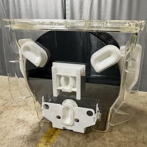
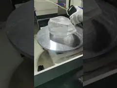
12 Inch Semiconductor Silicon Wafer Prime Test Dummy Wafers
Brand Name:BonTek
Certification:ISO:9001, ISO:14001
Model Number:Silicon Wafer
Minimum Order Quantity:25 Pieces
Delivery Time:1 - 4 weeks
Payment Terms:T/T
Contact Now
Add to Cart
Verified Supplier
Location:
Hangzhou Shanghai China
Address:
Room 1106, CIBC, No.198 Wuxing Rd, Hangzhou, P.R.China
Supplier`s last login times:
within 30 hours
Product Details
Company Profile
Product Details
12 inch Silicon Wafer Prime Test Dummy Wafers
Silicon wafer is a material used for producing semiconductors, which can be found in all types of electronic devices that improve the lives of people. Silicon comes second as the most common element in the universe; it is mostly used as a semiconductor in the technology and electronic sector.
There are various methods used in silicon fabrication counting the horizontal Bridgeman method, horizontal gradient freeze method, vertical gradient freeze, vertical Bridgeman method and the Czochralski pulling method.
The Silicon wafer is the main element in integrated circuits. Simply put, integrated circuits are a composite of a variety of electronic elements that are brought together to perform a particular function.
Silicon is the key platform for semiconductor gadgets. A wafer is just but a thin slice of the semiconductor material that acts as a substratum for microelectronic devices fitted in and above the wafer.
SEMI Standard | 2" (50.8mm) | 3" (76.2mm) | 4" (100mm) | 5" (125mm) | 6" (150mm) | 8" (200mm) | 12" (300mm) |
|---|---|---|---|---|---|---|---|
Diameter | 50.8 ± 0.38mm | 76.2 ± 0.63mm | 100 ± 0.5mm | 125 ± 0.5mm | 150 ± 0.2mm | 200 ± 0.2mm | 300 ± 0.2mm |
Thickness | 279 ± 25µm | 381 ± 25µm | 525 ± 20 µm or 625 ± 20µm | 625 ± 20µm | 675 ± 20µm or 625 ± 15µm | 725 ± 20µm | 775 ± 20µm |
Type | P, N or Intrinsic | ||||||
Dopant | B, Ph, As or Undoped | ||||||
Orientation | <100>, <111>, <110> | ||||||
Rsistivity | 0.001 – 300 ohm/cm | ||||||
Primary Flat Length | 15.88 ± 1.65mm | 22.22 ± 3.17mm | 32.5 ± 2.5mm | 42.5 ± 2.5mm | 57.5 ± 2.5mm | Notch | Notch |
Secondary Flat Length | 8 ± 1.65mm | 11.18 ± 1.52mm | 18 ± 2.0mm | 27.5 ± 2.5mm | 37.5 ± 2.5mm | NA | NA |
Surface Finish | SSP, DSP, Etched, or Lapped | ||||||
Thermal Oxide On Both Sides Of Wafer
Film thickness: 100Å – 10µm on both sides
Film thickness Tolerance: Target ±5%
Film stress: - 320±50 MPa Compressive
Thermal Oxide On Single Side Of Wafer
Film thickness: 100Å – 10,000Å on both sides
Film thickness Tolerance: Target ±5%
Film stress: -320±50 MPa Compressive
Acceptance Check
1. The product is fragile. We have adequately packed it and labeled it fragile. We deliver through excellent domestic and international express companies to ensure transportation quality.
2. After receiving the goods, please handle with care and check whether the outer carton is in good condition. Carefully open the outer carton and check whether the packing boxes are in alignment. Take a picture before you take them out.
3. Please open the vacuum package in a clean room when the products are to be applied.
4. If the products are found damaged during courier, please take a picture or record a video immediately. DO NOT take the damaged products out of the packaging box! Contact us immediately and we will solve the problem well.


12 Inch Semiconductor Silicon Wafer Prime Test Dummy Wafers
Inquiry Cart
0