
Add to Cart
FR4 HDI 10 Layer Pcb Fabrication 1.6mm Automated Pcb Assembly
HDI PCB Board PCB Fabrication Service Automated PCB Assembly 10
Layer PCB Low Volume Circuit Board Assembly
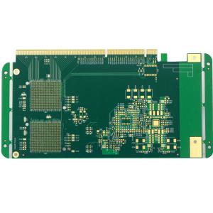
10L 1+N+1 HDI Printed Circuit Board
HDI PCB are abbreviation of high density interconnect printed
circuit boards, they are characterized by finer lines, closer
spaces, and more dense wiring.
For HDI boards own higher circuit density than traditional circuit
boards, its designs can include smaller through holes and capture
pads, and also higher connection pad density. They are widely used
to reduce the weight and overall dimensions of products, as well as
to enhance the electrical performance of the device.
HDI boards are applied to wide range of industries, like digital
devices, smartphones and tablets, automobiles, aircraft and other
vehicles products.
HDI Board Stack-up:
1+N+1 with laser microvia and mechanical buried core via. The “1”
represents “build-up” or sequential lamination on each side of the
core.
i+N+i (i>=2) PCBs contain 2 or more “build-up” of high-density interconnect
layers. Microvias on different layers can be staggered or stacked.
Copper filled stacked microvia structures are commonly seen in
challenging designs.
HSX products cover 1~32L FR-4 PCB, IMS PCB,HDI Boards, high
frequency PTFE boards and Rigid-flex boards etc. It provides
flexible quick turn production services (12 hours to72 hours), as
well as small volume to big volume PCB manufacturing. Products are
widely used in high-tech fields such as communications, power
supplies, computer networks, digital products, industrial control,
science and education, medical devices, and aerospace. HSX owns
high-educated and experienced team and advanced production
equipment.
| PCB Layer | 12L 1+N+1 | PCB material | FR-4, S1000-2 |
| Copper thickness | 1oz inner base, 1oz finished copper | PCB thickness | 1.60MM |
| Min. hole size | 0.15mm | Min.PCB track/gap: | 3mil |
| PCB solder mask | Green | PCB silkscreen | White |
| PCB surface finished | Immersion Gold 2u | PCB outline | Rout/V-CUT |
| Application | FR-4, Rogers | ||
| Special requirement: | min. via hole size 0.15mm/impedance control | ||
FAQ:
Q1:Are you a factory or trade company?
A: Yes, we are the factory, we have independent quick turn
prototype PCB manufacturing & big volume PCB production lines.
Q2:What kind of PCB file format can you accept for production?
A: Gerber, PROTEL 99SE, PROTEL DXP, POWER PCB, CAM350, ODB+(.TGZ)
Q3:Are my PCB files safe when I submit them to you for
manufacturing?
A: We respect customer's copyright and will never manufacture PCB
for someone else with your files unless we receive written
permission from your side, nor we'll share these files with any
other 3rd parties. And we could sign NDA with client if necessary.
Q4:If we have no PCB file/Gerber file, only have the PCB sample,can
you produce it for me?
A: Yes,we could help you to clone the PCB. Just send the sample PCB
to us, we could clone the PCB design and work out it.
Q5:What is your standard lead time for PCB?
A: Sample/prototype(less than 3sqm):
1-2 Layers: 3 to 5working days (fastest 24hours for quick turn
services)
4-8 Layers: 7~12 working days (fastest 48hours for quick turn
services)
Mass production (less than 200sqm):
1-2 Layers:7 to 12 working days
4-8 Layers:10 to 15 working days
Q6:How will you usually ship the PCB?
A: Usually for small packages, we will ship the boards by
DHL,UPS,FedEx door to door service, we could use your shipping
account to do collection or use our account to ship in DDU (import
duty unpaid) delivery term.
For heavy goods more than 300kg, we may ship your PCB boards by
ship or by air to save freight cost. Of course, if you have your
own forwarder, we may contact them for dealing with your shipment.
Q7:What is your minimum order quantity?
A: No MOQ.The quantity will only affect the price. Please contact
us for RFQ.
Q8:Could you provide PCB Assembly services and components sourcing?
A: Yes, we could also provide components sourcing and PCB Assembly
services as well as box build if request.
Q9. How to get quick quotation?
Please provide gerber file and details of the board(including
layer, board thickness, copper thickness, surface treatment, solder
mask and silkscreen color, special request if any, demand quantity,
etc)
sample:
| PCB Type | 4L multilayer PCB |
| Surface finished | LF-HASL |
| Base material | FR4, TG170 |
| Copper thickness | 1oz inner base, 1oz finished copper |
| PCB solder mask | Green for both sides |
| PCB silkscreen | White for both sides |
| Special requirement | Resin plugged hole/plating edge, gold finger thickness 30u" |