
Add to Cart
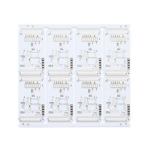
FR4 IT180A 10 Layer HDI PCB Board
HDI PCB Board 10 Layer PCB Board Prototype Circuit Board PCB Manufacturing PCB Board Manufacturing
10L 1+N+1 HDI Boards
HDI PCB means high density interconnect printed circuit boards,
they are characterized by finer lines, closer spaces, and more
dense wiring.
Due to its higher circuit density than traditional circuit boards,
HDI PCB designs can include smaller through holes and capture pads,
as well as higher connection pad density. HDI PCB is widely used to
reduce the weight and overall dimensions of products, as well as to
enhance the electrical performance of the device.
high frequency pcb HDI Board Stack-up:
1+N+1 with laser microvia and mechanical buried core via. The “1”
represents “build-up” or sequential lamination on each side of the
core.
i+N+i (i>=2) PCBs contain 2 or more “build-up” of high-density
interconnect layers. Microvias on different layers can be staggered
or stacked. Copper filled stacked microvia structures are commonly
seen in challenging designs.
HSX products cover 1~32L FR-4 PCB, IMS PCB,HDI Boards, high frequency PTFE boards and Rigid-flex boards etc. It provides flexible quick turn production services (12 hours to72 hours), as well as small volume to big volume PCB manufacturing.Products are widely used in high-tech fields such as communications, power supplies, computer networks, digital products, industrial control, science and education, medical devices, and aerospace.
| PCB Layer | 10L | PCB material | FR4 IT180A |
| Copper thickness | 1/H/H/H/H/H/H/H/H/1OZ | PCB thickness | 1.0MM |
| Min. hole size | 0.20mm | Min.PCB track/gap: | 4/6mil |
| PCB solder mask | White | PCB silkscreen | Black |
| PCB surface finished | Immersion Gold | PCB outline | Routing/V-CUT |
| Application | industrial control | ||
| Special requirement: | HDI Buried vias and blind vias, one step stack up /impedance control/resin filled and plated over | ||
FAQ:
Q1:Could you provide PCB Assembly services and components sourcing?
A: Yes, we could also provide components sourcing and PCB Assembly
services as well as box build if request.
Q2:Which countries have you worked with?
A:USA, Canada, Italy, Germany, UK, Spain, France, Russia, Iran,
Turkey, Czech Republic,Austria, Australia, Brazil, Japan, India
etc.
Q3:Will our PCB files be checked.
A: Yes. Your data will be checked by our Engineers Team. If we find
any technical issues or have any inquires, we will contact you and
solve the problems together.
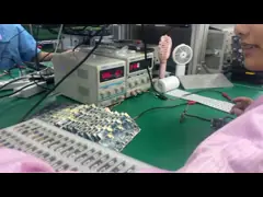
Q4: Does our product will be tested before shipment.
A: Yes. We could provide Function Circuit Testing if you provide us
the testing methods.
Q5:Which payment method do you accept?
A: Wire Transfer(T/T), Letter of Credit(L/C), or Paypal( Paypal is
only for small value less than 500usd)