Add to Cart
RoHS Multilayer High Frequency PCB 4 Layer Green Solder Mask Immersion Gold
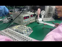
High Frequency PCB Multilayer PCB Board Four Layer Green High Frequency Prined Circuit Board
Four Layer Green High Frequency Prined Circuit Board
High-frequency PCBs usually provide a frequency range from 500MHz
to 2 GHz, which can meet the needs of high-speed PCB designs,
microwave, radio frequency, and mobile applications. When the
frequency is above 1 GHz, we can define it as high frequency.
The complexity of electronic components and switches is continually
increasing nowadays and need faster signal flow rates. So, higher
transmission frequencies are required. High-frequency PCBs help a
lot when integrating special signal requirements into electronic
components and products with advantages like high efficiency, and
fast speed, lower attenuation, and constant dielectric properties.
High Frequency (HF) PCB is used to transmit electromagnetic waves
in the frequency of GHz with minimal loses in the variety of
applications, including mobile, microwave, radio frequency (RF) and
high-speed design applications. Hence, printed circuit boards with
some specific characteristics are used to transmit these
electromagnetic waves. Several parameters are taken into
considerations while designing a PCB for high frequency
applications. custom pcb board
A high frequency PCB can meet your needs when incorporating a
special signal requirement into your electronic devices and
products. These higher transmission frequencies are capable of
supporting the faster signal flow rates that are a necessity in
today’s increasingly complex electronic switches and other
components.
| Feature | Capability |
| Quality Grade | Standard IPC 2 |
| Number of Layers | 2- 24layers |
| Material | ROGERS, TACONIC, ARLON, FR4, |
| Board Size | Min 5mm x 5mm | Max 500mm x 745mm |
| Board Thickness | 0.2mm - 4.0mm |
| Copper Weight(Finished) | 0.5oz - 2oz |
| Min Tracing/Spacing | 3mil/3mil |
| Solder Mask Color | Green, White, Blue, Black, Red, Yellow... |
| Silkscreen Color | White, Black, Yellow... |
| Surface Finish | Electroless nickel/immersion gold (ENIG) - RoHS |
| Immersion silver - RoHS | |
| Immersion tin - RoHS | |
| Min Annular Ring | 0.1mm |
| Min Drilling Hole Diameter | 0.15mm |
| Other Techniques | Peelable solder mask |
| Gold fingers | |
| Carbon oil | |
| Countersink holes |
FAQ:
Q1:Are you a factory or trade company?
A: Yes, we are the factory, we have independent quick turn
prototype PCB manufacturing & big volume PCB production lines.
Q2:How about your PCB factory production capacity?
A: Our monthly production capacity is 50,000 square meter/month and
5000types/month.
Q3:If we have no PCB file/Gerber file, only have the PCB sample,can
you produce it for me?
A: Yes,we could help you to clone the PCB. Just send the sample PCB
to us, we could clone the PCB design and work out it.
Q4:How will you usually ship the PCB?
A: Usually for small packages, we will ship the boards by
DHL,UPS,FedEx door to door service, we could use your shipping
account to do collection or use our account to ship in DDU (import
duty unpaid) delivery term.
For heavy goods more than 300kg, we may ship your PCB boards by
ship or by air to save freight cost. Of course, if you have your
own forwarder, we may contact them for dealing with your shipment.
Q5:What is your standard lead time for production?
A: Sample/prototype(less than 3sqm):
1-2 Layers: 3 to 5working days (fastest 24hours for quick turn
services)
4-8 Layers: 7~12 working days (fastest 48hours for quick turn
services)
Mass production (less than 200sqm):
1-2 Layers:7 to 12 working days
4-8 Layers:10 to 15 working days