Add to Cart
2 Layer Flex PCB Board 0.5mm 3mil ENIG Quick Turn PCB Assembly
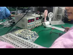
Flex PCB Board 2 Layer Flexible PCBA Flex PCB Assembly Quick Turn PCB Assembly Flexible Pcb Assembly
2 Layer Flexible PCBA
Flexible printed circuits are circuit boards that have the ability to bend or twist. From this assertion, it is obvious that they are distinguished by a flexible construction. That is why electronic engineers and designers use them in applications that demand for their qualities. They are also referred to as flex circuits and are mostly used in small electronic applications. Since they are characterized by their ability to bend, flexible printed circuits are made of flexible substrate such as polyimide. Another important quality of flexible printed circuits is that they have superior heat dissipation than printed circuit boards. It is this quality that makes it possible for the electronics that use it to stay in quality condition for a long time.
HSX products cover 1~32L FR-4 PCB, IMS PCB,HDI Boards, high frequency PTFE boards and Rigid-flex boards etc. It provides flexible quick turn production services (12 hours to72 hours), as well as small volume to big volume PCB manufacturing.Products are widely used in high-tech fields such as communications, power supplies, computer networks, digital products, industrial control, science and education, medical devices, and aerospace.
| FPC Technology Capability | |||
| Attribute (All dimensions are mils unless otherwise specified) | Mass Production (Yield≥ 80%,Cpk≥1.33) | Small Amount(Yield≥60%, Key Specification Yield≥80% | Sample |
| FPC(yes/no) | yes | yes | yes |
| Layer count/Structure, Max. | 2 | 4 | 6 |
| Size(L×W), Max. | 550mm*250mm | 550mm*250mm | 700mm*250mm |
| Nominal thickness (mm) | 0.1~0.5 | 0.1~0.5 | 0.1~0.8 |
| Thickness tolerance | ±10%(>0.3mm)/±0.03mm(≤0.3mm) | ±10%(>0.3mm)/±0.03mm(≤0.3mm) | ±10%(>0.3mm)/±0.03mm(≤0.3mm) |
| Surface finish type | ENIGENEPIGOPSI-SilverI-Tin HASLHard Gold | ENIGENEPIGOPSI-SilverI-Tin HASLHard Gold | ENIGENEPIGOPSI-SilverI-Tin HASLHard Gold |
| Soft ENIG(yes/no) | no | no | no |
| Base material type | PI | PI | PILCPTK |
| Coverlay thickness (um) | 28/50/60/80 | 28/50/60/80 | 28/50/60/80 |
| Adhesive thickness (um) | 25/40/50/65 | 25/40/50/65 | 25/40/50/65 |
| Copper thickness, Min./Max. (um) | 12-70 | 12-70 | 12-70 |
| Base material thickness, Min./Max. (um) | 25-75 | 25-75 | 25-100 |
| Mechanical drilled thru-hole size (DHS), Min. | 0.15 | 0.15 | 0.15 |
| Plating aspect ratio, Max. | 3:1 | 3:1 | 5:1 |
| Pad size, Min. | With through hole:0.4mm Without through hole:0.2mm | With through hole:0.4mm Without through hole:0.2mm | With through hole:0.3mm Without through hole:0.2mm |
| Pad size tolerance | 20% | 20% | 10% |
| Pad to pad space, Min. | 4mil | 4mil | 4mil |
| Pad to outline tolerance | ±3mil | ±3mil | ±2mil |
| Pattern location accurancy | ±3mil | ±3mil | ±2mil |
| Pattern location accurancy from top side to bottom | ±3mil | ±3mil | ±2mil |
| Laser via hole diameter/pad, Min. | 4/12mil | 4/10mil | 4/10mil |
| Outerlayer(Hoz+plating) line width/space, Min. | 3/3mil | 3/3mil | 2/2mil |
| Innerlayer(Hoz) line width/space, Min. | 3/3mil | 3/3mil | 2/2mil |
| Inner line width tolerance | ±10% | ±10% | ±10% |
| Outerlayer registration, Min. (Pad diameter = DHS + X) | DHS + 8 | DHS + 8 | DHS + 6 |
| Innerlayer registration, Min. (Pad diameter = DHS + X)(L≤4 layer) | DHS + 10 | DHS + 10 | DHS + 8 |
| Laser via hole pitch, Min. | 0.40mm | 0.40mm | 0.35mm |
| Mechanical hole pitch, Min. | 0.50mm | 0.50mm | 0.40mm |
| Drilled hole position tolerance | ±2mil | ±2mil | ±2mil |
| Hole size tolerance | ±2mil | ±2mil | ±2mil |
| Location accurancy from tooling hole(PTH&NPTH) to pad | ±3mil | ±3mil | ±2mil |
| Location accurancy from tooling hole(PTH&NPTH) to outline | ±3mil | ±3mil | ±2mil |
| Outline size tolerance | ±2mil | ±2mil | ±2mil |
| LPI registration/dam, Min. | 2mil/4mil | 2mil/4mil | 2mil/3mil |
| LPI dam on CVL | 8mil | 8mil | 8mil |
| Coverlay open window/dam | Φ0.5mm/0.3mm | Φ0.5mm/0.3mm | Φ0.3mm/0.2mm |
| Coverlay registration/Resin flow | 4mil | 4mil | 2mil |
| Stifferness material | FR4/PI/Steel | FR4/PI/Steel | FR4/PI/Steel |
| Stifferness dam, Min. | 12mil | 12mil | 8mil |
| Stifferness registration/Resin flow | 8mil/4mil | 8mil/4mil | 4mil/2mil |
| Impedance tolerance | 10% | 10% | 5% |
| Thermal reliability(LPI, FCCL, CVL) | 288°/10s/3times | 288°/10s/3times | 288°/10s/3times |
| Qualified material and structure UL | PI | PI | PI |
FAQ:
Q1:Are you a factory or trade company?
A: Yes, we are the factory, we have independent quick turn
prototype PCB manufacturing & big volume PCB production lines.
Q2:What kind of PCB file format can you accept for production?
A: Gerber, PROTEL 99SE, PROTEL DXP, POWER PCB, CAM350, ODB+(.TGZ)
Q3:Are my PCB files safe when I submit them to you for
manufacturing?
A: We respect customer's copyright and will never manufacture PCB
for someone else with your files unless we receive written
permission from your side, nor we'll share these files with any
other 3rd parties. And we could sign NDA with client if necessary.
Q4:If we have no PCB file/Gerber file, only have the PCB sample,can
you produce it for me?
A: Yes,we could help you to clone the PCB. Just send the sample PCB
to us, we could clone the PCB design and work out it.
Q5:What is your standard lead time for PCB?
A: Sample/prototype(less than 3sqm):
1-2 Layers: 3 to 5working days (fastest 24hours for quick turn
services)
4-8 Layers: 7~12 working days (fastest 48hours for quick turn
services)
Mass production (less than 200sqm):
1-2 Layers:7 to 12 working days
4-8 Layers:10 to 15 working days
Q6:What payment do you accept ?
A: Wire Transfer(T/T) or Letter of Credit(L/C) or Paypal(only for
small value less than 500usd)