
Add to Cart
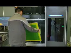
laser direct imaging (LDI) system solutions PCB Solder Mask
Advantages of LDI over photo processing
When creating the photo tool for generating the image on the board, it needs to have multiple steps for the traditional photo processes. For years, there are a lot of challenges for the PCB manufacturer. And LDI have a lot of advantages:
Quality - in the past, the problem of photo films have led to imperfect images because of inherent susceptibility to fluctuations in temperate or humidity. Laser images bring about more accurate and consistent images, and clear up any film-related defects.
There have accurate positioning and improved resolution. As well as more precise image lines, spaces, and image alignment.
When the photo method is providing the most accurate transfer of images to the boards, it needs to have temperature and humidity controlled environments. LDI reduces the effect of environment on the resulting images, and eliminates the impacts of light refraction inherent with photo processing techniques.
LDI manufacturing has particular advantages under the circumstances of short runs or quick turn-around, and it’s impractical for the creation of artwork and setup of photo tool methods. When it comes to tight registration and close tolerances, LDI is also an important factor.
Nowadays, taking photo technology as a practical tool in creating PCB images because the customers have the demands for smaller, lighter, high-density PCBs.
| Specification/model | DPX230 |
| Application | PCB,HDI,FPC (inner layer,outer layer,anti-welding) |
| Resolution (mass production) | 30um |
| Capacity | 30-40S@18"*24" |
| Exposure Size | 610*710mm |
| Panel thickness | 0.05mm-3.5mm |
| Alignment Mode | UV-Mark |
| Alignment capability | Outer layer±12um;Inner laye±24um |
| Line width tolerance | ±10% |
| Deviation increase and decrease mode | Fixed increase and contraction, automatic increase and contraction, interval increase and contraction, partition alignment |
| Laser type | LD Laser,405±5nm |
| File format | Gerber 274X;ODB++ |
| Power | 380V three-phase alternating current, 6.4kW,50HZ, voltage fluctuation range + 7% ~-10% |
| Condition | Yellow light room; Temperature 22°C ± 1°C; Humidity 50% ± 5%;
Cleanliness level 10000 and above; Vibration requirements to avoid violent vibration near the equipment |
How does laser direct imaging ( LDI ) work?
Laser direct imaging needs a PCB with the photo-sensitive surface
that is positioned under a computer controlled laser. And then the
computer is creating the image on the board with the light of
laser. A computer scans the board surface into a raster image,
matching the raster image to a pre-loaded CAD or CAM design file
that includes the specifications for the necessary image intended
for the board, the laser is used for directly creating the image on
the board.
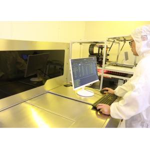
About us
We are an innovative supplier of various PCB laser direct imaging
(LDI) system solutions. Our system product portfolio ranges from
LDI system configurations for high-mix and emerging PCB niche
applications to fully automated LDI system solutions for mass
production environments.