
Add to Cart
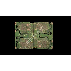
10Layer anylayer HDI PCB for 5G mobile phone motherboard
Any layer of interconnect board products can be applied to mobile communication terminals, which integrates a variety of circuits, enabling mobile terminals to handle complex tasks and have rich communication methods. With the development of communication technologies, mobile terminals have become modern Internet services. The main platform.
Printed circuit board, the heart of every electronic device, is important not only because it allows the electrical connections between the various components, but also because it carries digital and analog signals, high frequency data transmission signals and power supply lines. With the introduction of 5G technology, what will the new demands and requirements that PCBs have to meet? Compared to 4G, the imminent large-scale deployment of 5G network will force designers to rethink the design of PCBs for mobile, IoT and telecommunications devices. The 5G network will be characterized by high speed, wide bandwidth and low latency, all aspects that will require careful PCB design in order to support the new high-frequency features.
1. Product application
Any layer of interconnect board products can be applied to mobile communication terminals, which integrates a variety of circuits, enabling mobile terminals to handle complex tasks and have rich communication methods. With the development of communication technologies, mobile terminals have become modern Internet services. The main platform.
2 . Specifications:
| Name | 10Layer anylayer HDI PCB for 5G mobile phone motherboard |
| Layer | 10 |
| Quality Grade | IPC 6012 Class 2,IPC 6012 Class 3 |
| Material | EM370 |
| Min Track/Spacing | 75um/100um |
| Drilling Size | 100um |
| Solder Mask | Green |
| Silkscreen | White |
| Surface Finish | Immersion gold |
| Finished Copper | 1/3OZ |
| Production time | 10-21 working days |
| Lead time | 2-3 days |
PCBs for high frequency applications require to be subjected to automatic inspection procedures, both optical (AOI) or performed through ATE. These procedures allow to enormously increase the quality of the product, highlighting possible errors or inefficiencies of the circuit. The recent progress made in the field of automatic inspection and testing of PCBs has led to significant time savings and reduced costs associated with manual verification and testing. The use of new automated inspection techniques will help overcome the challenges imposed by 5G, including global impedance control in high frequency systems. Increased adoption of automated inspection methods also allows for consistent performance with high production rates.

