
Add to Cart
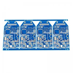
Multilayer HDI Quick Term Printed Circuit Board &PCBA Rigid Flexible PCB
As consumer demands change, so must technology. By using HDI technology, designers now have the option to place more components on both sides of the raw PCB. Multiple via processes, including via in pad and blind via technology, allow designers more PCB real estate to place components that are smaller even closer together. Decreased component size and pitch allow for more I/O in smaller geometries. This means faster transmission of signals and a significant reduction in signal loss and crossing delays.
High-density interconnect, or HDI, circuit boards are printed circuit boards with a higher wiring density per unit area than traditional printed circuit boards. In general, HDI PCBs are defined as PCBs with one or all of the following: microvias; blind and buried vias; built-up laminations and high signal performance considerations. Printed circuit board technology has been evolving with changing technology that calls for smaller and faster products. HDI boards are more compact and have smaller vias, pads, copper traces and spaces. As a result, HDIs have denser wiring resulting in lighter weight, more compact, lower layer count PCBs. Rather than using a few PCBs in a device, one HDI board can house the functionality of the previous boards used.
Specifications:
| Technical Capacity | |||
| ltem | Rigid PCB | Flexible PCB | Rigid-Flex PCB |
| Max Layer | 24L | 8L | 20L |
| Inner Layer Min Trace/Space | 3/3mil | 3/3mil | 3/3mil |
| Out Layer Min Trace/Space | 3/3mil | 3.5/4mil | 3.5/4mil |
| Inner Layer Max Copper | 6oz | 2oz | 6oz |
| Out Layer Max Copper | 6oz | 2oz | 3oz |
| Min Mechanical Driling | 0.15mm | 0.1mm | 0.15mm |
| Min Laser Drilling | 0.1mm | 0.1mm | 0.1mm |
| Max Aspect Ratio(Mechanical Driling) | 20:01 | 10:01 | 12:01 |
| Max Aspect Ratio(Laser Drilling) | 1:01 | / | 1:01 |
| Press Fit Hole Ttolerance | ±0.05mm | ±0.05mm | ±0.05mm |
| PTH Tolerance | ±0.075mm | ±0.075mm | ±0.075mm |
| NPTH Tolerance | ±0.05mm | ±0.05mm | ±0.05mm |
| Countersink Tolerance | ±0.15mm | ±0.15mm | ±0.15mm |
| Board Thickness | 0.4-8mm | 0.1-0.5mm | 0.4-3mm |
| Board Thickness Tolerance(<1.0mm)<> | ±0.1mm | ±0.05mm | ±0.1mm |
| Board Thickness Tolerance(≥1.0mm) | ±10% | / | ±10% |
| Min Board Size | 10*10mm | 5*10mm | 10*10mm |
| Max Board Size | 620*1200mm | 480*540mm | 480*540mm |
| Contour Tolerance | ±0.1mm | ±0.05mm | ±0.1mm |
| Min BGA | 7mil | 7mil | 7mil |
| Min SMT | 7*10mil | 7*10mil | 7*10mil |
| Min Solder Mask Clearance | 1.5mil | 3mil | 1.5mil |
| Min Solder Mask Dam | 3mil | 8mil | 3mil |
| Min Legend Width/Height | 4/23mil | 4/23mil | 4/23mil |
| Strain Fillet Width | / | 1.5±0.5mm | 1.5±0.5mm |
| Bow &Twist | 0.70% | / | 0.70% |
Our advantage:
A. Very competitive price
B. Fast lead time from 12 hours
C. Perfect service and good relation ship with customer
D. Good quality. Welcome all kinds OEM ODM PCB order!
Advantages:
The most common reason for using HDI technology is a significant increase in packaging density. The space obtained by finer track structures is available for components. Besides, overall space requirements are reduced will result in smaller board sizes and fewer layers.
Usually FPGA or BGA are available with 1mm or less spacing. HDI technology makes routing and connection easy, especially when routing between pins.
