1oz Pcb Fabrication Service , Bare Pcb Board Pcb Manufacturing Assembly

Brand Name:CKS
Certification:ISO9001
Model Number:CKS-Customized
Minimum Order Quantity:1 Piece/Pieces
Delivery Time:90-120 work days
Payment Terms:L/C, Western Union, MoneyGram, T/T
Contact Now

Add to Cart

Active Member
Location: Shenzhen China
Address: FL.3-4,Blog.K,Jinchangda Tech Park,Guanlan St.,Longhua Dist.,Shenzhen,China
Supplier`s last login times: within 13 hours
Product Details Company Profile
Product Details

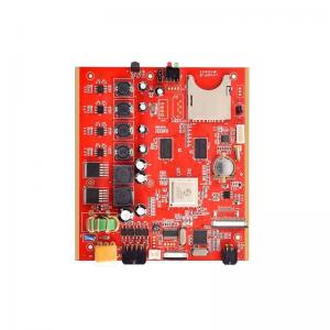
Pcb Fabrication Service Bare Pcb Board Pcb Manufacturing Assembly


Files and Requirment for PCB,PCBA quotation:

  • A BOM (Bill of Materials) with reference designators: component description, manufacturer’s name and part number.
  • PCB Gerber files.
  • A PCB fabrication drawing and PCBA assembly drawing.
  • Test procedures.
  • Any mechanical restrictions such as assembly height requirements
  • PCB board manufacture and PCBA service:
    • o PCB board made, circuit board parts purchased by us
    • o Electronic testing circuit board or PCBA
    • o Fast delivery, anti-static package
    • o RoHS Directive-compliant, lead-free
    • o One stop service from PCB design, PCB layout, PCB manufacture, components purchasing, PCB assembly, test, packing and PCB delivery
    • o Eleectronic manufacturing service
  • Detailed terms for PCB assembly:
    • o Technical requirement:
      • § Professional surface-mounting and through-hole soldering technology
      • § Various sizes like 1206, 0805, 0603 components SMT technology
      • § ICT (In Circuit Test), FCT (Functional Circuit Test) technology
      • § PCB assembly with UL, CE, FCC, RoHS approval
      • § Nitrogen gas reflow soldering technology for SMT
      • § High standard SMT and solder assembly line
      • § High density interconnected board placement technology capacity
    • o Quote requirement:
      • § Gerber file and Bom list
      • § Clear pics of pcba or pcba sample for us
      • § Test method for PCBA
    • o PCB specification:
      • § Layer: 1 to 12 layers
      • § Material: FR-4, CEM-1, CEM-3, Hight TG, FR4 halogen free, FR-1, FR-2,Aluminum etc.
      • § Max. finished thickness: 0.2 to 4.0mm (0.02 ~ 0.25)
      • § Max. finished board side: 500 x 500mm (20 x 20”)
      • § Min. drilled hole size: 0.25mm (10mil)
      • § Min. line width: 0.10mm (4mil)
      • § Min. line spacing: 0.10mm (4mil)
      • § Surface finish/treatment: HALS/HALS lead free, chemical tin, chemical gold, immersion gold, plating gold
      • § Copper thickness: 0.5 to 3.0 oz
      • § Solder mask color: green/black/white/red/blue
      • § Inner packing: plastic bag
      • § Outer packing: standard carton packing
      • § Hole tolerance: PTH: ±0.076, NTPH: ±0.05
      • § Certificate: UL, ISO 9001, ISO 14001, RoHS,UL
      • § Profiling punching: routing, V-cut, beveling
      • § Providing OEM service to all sorts of printed circuit board assembly

Detailed Terms for PCB Assembly

Technical RequirementProfessional Surface-mounting and Through-hole soldering Technology
Various sizes like 1206,0805,0603 components SMT technology
ICT(In Circuit Test),FCT(Functional Circuit Test) technology
PCB Assembly With CE,FCC,Rohs Approval
Nitrogen gas reflow soldering technology for SMT
High Standard SMT&Solder Assembly Line
High density interconnected board placement technology capacity
Quote&Production RequirementGerber File or PCB File for Bare PCB Board Fabrication
Bom(Bill of Material) for Assembly,PNP(Pick and Place file) and Components Position also needed in assembly
To reduce the quote time, please provide us the full part number for each components,Quantity per board also the quantity for orders.
Testing Guide&Function Testing method to ensure the quality to reach nearly 0% scrap rate
OEM/ODM/EMS ServicesPCBA, PCB assembly: SMT & PTH & BGA
PCBA and enclosure design
Components sourcing and purchasing
Quick prototyping
Plastic injection molding
Metal sheet stamping
Final assembly
Test: AOI, In-Circuit Test (ICT), Functional Test (FCT)
Custom clearance for material importing and product exporting
Other PCB Assembly EquipmentsSMT Machine: SIEMENS SIPLACE D1/D2 / SIEMENS SIPLACE S20/F4
Reflow Oven: FolunGwin FL-RX860
Wave Soldering Machine: FolunGwin ADS300
Automated Optical Inspection (AOI): Aleader ALD-H-350B,X-RAY Testing Service
Fully Automatic SMT Stencil Printer: FolunGwin Win-5

Product Description
Product Name
PCBA customize
Surface Finishing
Gold Plating
Certificate
ROHS. ISO9001.
Pcb board material
Fr4 / Aluminum / Cu
Copper Thickness
0.5-3OZ
Board Thickness
0.8-2.0mm
Testing Service
Fly-probe/AOI/100%function Testing
PCB layer
SMT DIP Electronic Board

FR-4 Process capability
NOItemCraft Ability
1Surface FinishHASL,Immersion Gold,Gold Plating,OSP,Immersion Tin,etc
2Layer1-32 layers
3Min.Line Width4mil
4Min.Line Space4mil
5Min.Space between Pad to Pad3mil
6Min.Hole Diameter0.20mm
7Min.Bonding Pad Diameter0.20mm
8Max.Proportion of Drilling Hole and Board Thickness1:10
9Max.Size of Finish Board23inch*35inch
10Rang of Finish Board′s Thickness0.21-3.2mm

China 1oz Pcb Fabrication Service , Bare Pcb Board Pcb Manufacturing Assembly supplier

1oz Pcb Fabrication Service , Bare Pcb Board Pcb Manufacturing Assembly

Inquiry Cart 0